B-10
01/99
2N4220, 2N4220A, 2N4221, 2N4221A, 2N4222, 2N4222A
N-Channel Silicon Junction Field-Effect Transistor
• Mixers
• Oscillators
• VHF Amplifiers
• Small Signal Amplifiers
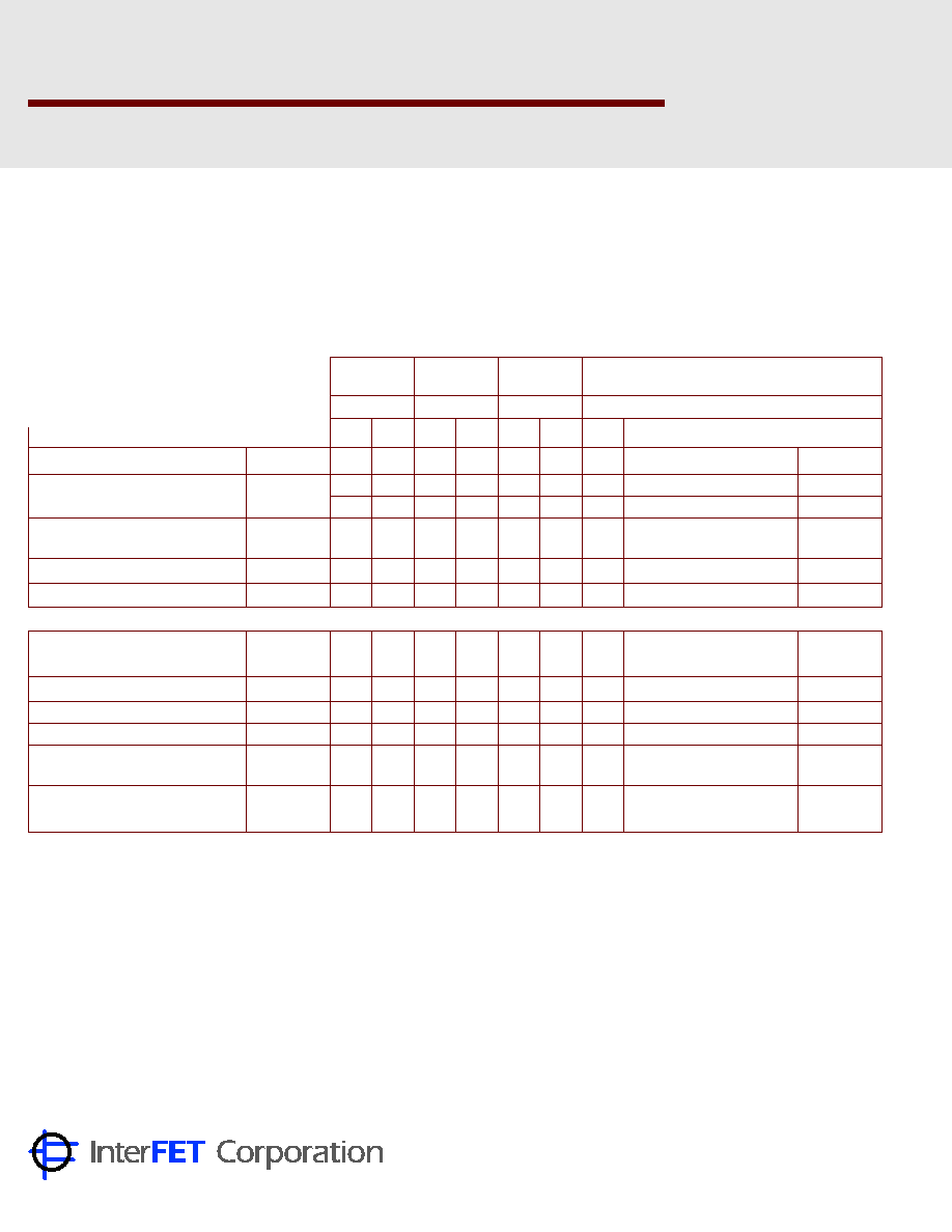
Absolute maximum ratings at T
A
= 25°C
Reverse Gate Source & Reverse Gate Drain Voltage
≠ 30 V
Continuous Forward Gate Current
10 mA
Continuous Device Power Dissipation
300 mW
Power Derating (to 150 ∞C)
2 mW/∞C
TO–72 Package
Dimensions in Inches (mm)
Pin Configuration
1 Source, 2 Drain, 3 Gate, 4 Case
2N4220
2N4221
2N4222
2N4220A
2N4221A
2N4222A
At 25∞C free air temperature:
NJ16
NJ16
NJ32
Process
Static Electrical Characteristics
Min
Max
Min
Max
Min
Max
Unit
Test Conditions
Gate Source Breakdown Voltage
V
(BR)GSS
≠ 30
≠ 30
≠ 30
V
I
G
= ≠ 1µA, V
DS
= ÿV
Gate Reverse Current
I
GSS
≠ 0.1
≠ 0.1
≠ 0.1
nA
V
GS
= ≠ 15V, V
DS
= ÿV
≠ 0.1
≠ 0.1
≠ 0.1
µA
V
GS
= ≠ 15V, V
DS
= ÿV
T
A
= 150∞C
Gate Source Voltage
V
GS
≠ 0.5
≠ 2.5
≠ 1
≠ 5
≠ 2
≠ 6
V
V
DS
= 15V, I
D
= ( )
(50)
(50)
(200) (200) (500) (500)
µA
Gate Source Cutoff Voltage
V
GS(OFF)
≠ 4
≠ 6
≠ 8
V
V
DS
= 15V, I
D
= 0.1 nA
Drain Saturation Current (Pulsed)
I
DSS
0.5
3
2
6
5
15
mA
V
DS
= 15V, V
GS
= ÿV
Dynamic Electrical Characteristics
Common Source Forward
g
fs
1000
4000
2000
5000
2500
6000
µS
V
DS
= 15V, V
GS
= ÿV
f = 1 kHz
Transconductance
Common Source Forward Transmittance
| Y
fs
|
750
750
750
µS
V
DS
= 15V, V
GS
= ÿV
f = 100 MHz
Common Source Output Conductance
g
os
10
20
40
µS
V
DS
= 15V, V
GS
= ÿV
f = 1 kHz
Common Source Input Capacitance
C
iss
6
6
6
pF
V
DS
= 15V, V
GS
= ÿV
f = 1 MHz
Common Source Reverse
C
rss
2
2
2
pF
V
DS
= 15V, V
GS
= ÿV
f = 1 MHz
Transfer Capacitance
Noise Figure
NF
2.5
2.5
2.5
dB
V
DS
= 15V, V
GS
= ÿV
f = 100 MHz
2N4220A, 2N4221A, 2N4222A
R
G
= 1 M
1000 N. Shiloh Road, Garland, TX 75042
(972) 487-1287
FAX
(972) 276-3375
www.interfet.com
Databook.fxp 1/13/99 2:09 PM Page B-10